
Thank you for visiting nature.com. You are using a browser version with limited support for CSS. To obtain the best experience, we recommend you use a more up to date browser (or turn off compatibility mode in Internet Explorer). In the meantime, to ensure continued support, we are displaying the site without styles and JavaScript.
Advertisement
Scientific Reports volume 15, Article number: 3396 (2025)
Metrics details
According to recent research, with the ever-increasing use of Internet of Things (IoT) devices, there has arisen an ever-growing need for high-performance yet low-power circuits that can efficiently process information. Quantum-dot Cellular Automata (QCA) has emerged as a promising alternative to conventional complementary metal-oxide-semiconductor (CMOS) technology due to its great potential in digital design at nanoscale levels on account of very low power consumption and very high processing speed. However, QCA circuits are inherently prone to faults due to variations in manufacturing processes and due to the influence of environmental factors. These faults degrade the performance of a QCA circuit considerably. Hence, fault tolerance is one of the major factors of consideration while designing a QCA circuit, particularly when the application requires very reliable and continuous operation, say in an IoT system. As such, this work presents a fault tolerant Carry Skip Adder (CSA) for QCA-based circuits. The fault tolerance of basic arithmetic components of IoT nodes performing tasks corresponding to the signal processing, control, and data manipulations is enhanced in the proposed architecture. The area occupied by a fault-tolerant full-adder circuit is 0.06 μm² and a clock cycle is 0.75; its core will be used in the CSA design. It realizes fault-tolerant multiplexers (MUX) and a majority gate, which gives the same result when there is a missing or extra single-cell fault. The most astonishing characteristic of this transistor-based CSA is its 85% tolerance for different types of failures. The CSA with three layers contains 1542 quantum cells, 4.75 clock phases, and occupies an area of 4.59 μm². It is compact and efficient architecture; therefore, it is very suitable for IoT applications where the area constraint and power efficiency are the key issues. The proposed CSA will increase the robustness and reliability of QCA-based digital circuits by integrating fault tolerance into its design such that the circuitry based on QCA can keep their functionality on even in fault-prone environments.
Superconductor technology utilizing metal-oxide compounds has gained extensive application in the production of digital circuits and chips. Similar to various methodologies, this approach entails a delicate balance between speed and power consumption. The constraints inherent in factors such as switching speed, scaling parameters, elevated lithography expenses, and thermal challenges suggest that complementary metal-oxide-semiconductor (CMOS) technology is approaching obsolescence. As a result of the impending limitations facing future CMOS advancements, numerous researchers are exploring alternative technologies as potential replacements1,2.
As a result, researchers are looking for new technologies, with Quantum-dot Cellular Automata (QCA) emerging as the most promising option3. QCA is a data representation and processing technology that makes use of the quantum properties of charged particles and the electrostatic interaction theory. QCA technology has much higher circuit density than traditional CMOS circuits, and its distinguishing features of fast switching speed and low power consumption place it at the forefront of technological innovation4,5. QCA, which is based on the concept of artificial semiconductor atoms, enables the fabrication of digital components on the nanoscale6. QCA technology has been used to successfully construct circuits such as fundamental logic gates, adders, multipliers, multiplexers, and memory. Numerous implementations in the development of QCA cellular structures have been shown, and their performance has been extensively evaluated7,8.
Nonetheless, this technology has certain downsides, the most noteworthy of which is its vulnerability to flaws. Due to the intrinsic vulnerability of QCA circuits to manufacturing flaws and external interruptions, fault tolerance is crucial in the field of QCA technology. Fault tolerance refers to a system’s ability to continue operating correctly in the event of faults or failures9. In QCA, many types of defects, such as missing cells, excess cells, rotated cells, or misplaced cells, can appear, causing significant interruptions in circuit performance and resulting in output errors. Fault tolerance in QCA circuits has become critical for encouraging stable and resilient functioning, effectively minimizing the negative impacts of manufacturing faults and environmental influences. By using fault-tolerant designs and procedures, QCA circuits are able to identify and correct defects, guaranteeing constant operation even in the event of failures7,10. Fault tolerance is a feature of QCA technology that extends the life of QCA-based devices by reducing the possibility of catastrophic failures and strengthening system resilience. It enables QCA circuits to reliably and precisely carry out their assigned responsibilities even when faced with a variety of failure conditions. The research and engineering community’s goal to improve the dependability, stability, and overall performance of QCA-based systems is reflected in the concerted effort to address fault tolerance in QCA. This will make QCA-based systems more appropriate for real-world applications where dependability and error-free operation are critical.
However, in contemporary times, the term “Internet” refers to a considerably larger range of devices than only personal computers connected to networks. Traditional microdevices, such as sensors and controllers, are constrained to performing domain-specific activities according to predefined criteria. By replacing these task-specific devices with microcomputers controlled by CPUs and outfitted with connection features, these “things” gain greater intelligence due to higher computational capabilities and information interchange enabled by Internet connectivity. As a result, these entities may do more complex activities than their prior capabilities permitted, and users can easily receive and handle data supplied by these entities by utilizing cloud services.
Creating fault-tolerant Carry Skip Adder (CSA) designs on the nano-scale QCA platform is critical for assuring accurate and dependable outcomes in Internet of Things (IoT) communications, even in the face of manufacturing flaws or environmental disruptions. Integration circuits are used in a variety of sectors, including the Internet of Things, mobile communication systems, surveillance systems, medical domains, wireless sensor networks, space applications, robotics, image vision, and others11. Adders are critical in these applications for ensuring optimal performance in terms of adding speed and power consumption. When building large circuits, it is critical to keep the design fault-tolerant in mind. Adder circuits, which are fundamental mathematical functions, are commonly used in microprocessors and digital signal processors to perform a variety of complicated arithmetic operations such as address calculation, division, and multiplication. Adders may meet a variety of needs, including fast speed and low power consumption. This kind of circuit is essential for enhancing the robustness and durability of QCA-based Internet of Things connections as well as lessening the effect of mistakes on outputs.
By employing fault-tolerant techniques and designs, the circuit can effectively detect and reduce errors, enabling precise and reliable IoT connections. Finally, the inclusion of a fault-tolerant circuit for CSA in QCA technology is intended to improve the reliability and efficacy of IoT communications. This paper fills a research vacuum by introducing a novel circuit for fault-tolerant CSA that uses reliable majority logic gates to replicate the desired functionality. The performance of the proposed circuit is then visualized by modeling it with QCADesigner-E.
The remaining parts of the paper are organized as follows: Sect. 2 includes an explanation of the fundamentals of QCA technology and IoT, as well as a review of related earlier work. Section 3 examines the proposed framework, while Sect. 4 examines the simulation findings. Section 5, the concluding section, summarizes the paper’s conclusion.
An overview of QCA fundamentals, clocking mechanisms, fault considerations, the IoT concept, and relevant research in this context will be presented.
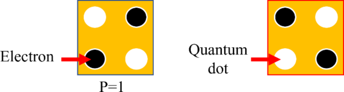
QCA’s core basic pieces are bistable cells made up of four quantum dots. Two free electrons are present in each cell and have the ability to tunnel between neighboring dots. Because of their electrostatic repulsion, these electrons preferentially occupy antipodal sites inside the cell12. As a result, two unique energetically advantageous electron arrangements occur, resulting in two possible configurations for the QCA cell: cell polarization P = + 1 and P= −1. This intrinsic duality serves as the foundation for encoding binary data in QCA, with P = + 1 representing logic “1” and P= −1 representing logic “0.” In greater detail, the idea of cell polarization governs the behavior of electrons within the QCA cell. This procedure demonstrates how easy and effective QCA is for expressing and working with binary data at the quantum level. In Fig. 1, the cell structure is displayed13,14.
Two types of QCA cell15.
The essential logic gates of QCA circuits and devices are the QCA wire, inverter, and majority voter, which have three and five inputs, respectively. The binary signal travels smoothly from input to output within a QCA wire, propelled by electrostatic interactions between cells. An intriguing approach is to use a 45° QCA wire instead of the typical 90° design16,17. The binary signal transmission in this case cyclically alternates between the two polarizations, demonstrating the flexibility and versatility of QCA circuitry. Figure 2 depicts two types of wire in QCA. Furthermore, QCA cells provide a dual duty by acting as the foundation for inverter logic gates. Figure 3(a) depicts inverter gate in QCA. These gates are made in an unconventional manner by connecting just the corners of the cells, resulting in an inversion of the electrostatic interaction owing to mismatched quantum dots. Unlike traditional gates, they are built by joining only the corners of the cells, which causes the electrostatic interaction to be flipped since the mismatched quantum dots between the cells correspond to different polarizations. This special feature highlights the creative possibilities and design adaptability of QCA circuits and offers an insight into unusual but effective methods of building logic gates17.
Two types of wire in QCA: (a) 45° QCA wire, and (b) 90° QCA wire18.
The QCA majority gate, a key component of QCA circuits, is programmed to perform a three-input logic function. Figure 3(b) shows a majority gate in QCA. The majority gate is predisposed to adopt the polarization of the majority among its nearby cells by leveraging the natural behavior of device cells19. This propensity stems from device cells’ proclivity to drift towards a ground state, coinciding with the majority polarization in their area. The motivation for this behavior is the pursuit of the lowest energy state, which causes the device cell to synchronize with the dominant polarization20,21. Furthermore, the QCA majority gate’s versatility extends to its capacity to act as both an AND gate and an OR gate. Fixing one of the three-input majority voter’s input terminals to polarity P= 1 for AND gate functionality and P = + 1 for OR gate functionality is necessary to provide this flexibility. Four quantum dots (QCA cells) are built around a core quantum cell in the building of the three-input majority voter itself, demonstrating the complexity of QCA design22.
QCA clocking is an important feature of QCA circuit design since it allows for synchronous and well-coordinated actions23. Unlike standard electrical circuits, QCA uses a timing mechanism based on the periodic reconfiguration of cell polarizations rather of a continuous clock signal. In most cases, the clocking process in QCA is accomplished by the controlled application of external disturbances or clocking signals. A clock signal generates a switch in the polarization states of QCA cells in QCA clocking, allowing binary information to be propagated. The clocking event initiates a series of cell contacts, resulting in the binary signal’s synchronized advancement across the circuit. One significant advantage of QCA clocking is its intrinsic parallelism, which allows numerous processes to perform concurrently. Initialization, application of the clock signal, calculation, and removal of the clock signal are the successive steps in the clocking process in QCA. The cells are first brought to a predetermined condition during initiation, and when the clock signal is added, the cells change polarizations. As the binary information travels through the circuit, computation takes place, and the clock signal is ultimately eliminated to finish the clocking cycle. To guarantee dependable and precise functioning, clocking characteristics including frequency, pulse length, and synchronization are carefully taken into account. Utilizing the special properties of QCA for effective and low-power computation in nanoscale devices requires QCA clocking. Figure 4shows clocking in QCA24.
Basic gaets in QCA: (a) Inverter gate in QCA, and (b) Majority gate in QCA.
Clocking in QCA.
QCA Different sorts of failures can have an influence on the dependable functioning of QCA circuits, each providing its own set of obstacles to circuit performance4,5. Here are some examples of frequent QCA flaws:
Missing cells: This happens when one or more QCA cells are missing from the circuit. As a result, the circuit has insufficient functioning and the flow of information is disrupted (Fig. 5 (a)).
Additional cells: The existence of additional cells in a QCA circuit. Can result in unanticipated interactions and affect the system’s intended function (Fig. 5 (b)).
Rotated cells: Cells that have been rotated, resulting in a change in charge alignment and orientation. Introduces mistakes, which may result in improper logic operations and jeopardize circuit correctness (Fig. 5 (c)).
Displaced cells: Errors brought on by incorrect alignment of QCA cells. disrupts the transmission of signals, which has an impact on the circuit’s overall performance (Fig. 5 (d)).
The susceptibility of QCA technology to modifications in cell layout is demonstrated by these different problems. For the purpose of creating fault-tolerant QCA circuits that can continue to function accurately and dependably in the face of such difficulties, it is essential to comprehend and resolve these problems.
QCA faults; (a) Missing cell, (b) Additional cell, (c) Rotated cell, and (d) Displaced cell.
The Internet of Things (IoT) is a novel idea that refers to a network of interconnected physical items, gadgets, or “things” integrated with sensors, software, and other technologies25. These items may gather, exchange, and share data with one another or with centralized systems via the internet or other communication networks11. The major objective of the Internet of Things is to allow these “smart” devices to interact, communicate, and make intelligent decisions without the need for direct human interaction.
A few essential components of the IoT idea are:
Devices that are Interconnected: The IoT encompasses a vast array of devices that are integrated with sensors and communication capabilities, such as commonplace items, machinery, appliances, cars, and more.
Data share: When IoT devices share data, a stream of information is created that may be examined and used for a number of objectives.
IoT devices are outfitted with sensors to gather information from their environment and, in certain situations, actuators to carry out certain tasks in response to the data gathered.
A key component of the IoT is connectivity, which enables objects to talk to one another and to centralized systems via the internet or other communication protocols.
Automation and intelligence: The IoT attempts to improve automation by allowing devices to make intelligent decisions based on the data they gather, resulting in increased efficiency and convenience.
Applications Across Industries: The IoT has a wide range of applications in a variety of industries, including healthcare, transportation, agriculture, manufacturing, and smart homes, all of which contribute to enhanced processes and services.
Ubiquitous Computing: The IoT extends computing capabilities beyond standard computing devices by integrating computer power into ordinary items and settings.
Overall, the IoTs notion symbolizes a paradigm change in how physical items and the digital world interact, opening up new avenues for creativity, efficiency, and increased quality of life26.
In the realm of QCA, numerous research endeavors have delved into various aspects, exploring applications like CSA. Some notable works in this domain include:
Al-Khafaji, et al.27 have proposed nano-scale CSA based on QCA technology. Researchers are exploring nano-scale CSA designs based on logic gate structures to improve system performance in terms of average power dissipation, area, and delay. The proposed ultra-low-power CSA reduces cell consumption by 64%, improves latency by 15%, and increases area by 85%. This design is the only way to reduce the latency of a ripple carry adder with low effort compared to a carry-look-ahead adder. But this circuit is not fault-tolerant.
Chen, et al.28 focused on the design of efficient QCA-based comparators, with a special interest in the rapidly growing IoT market, for which high-speed and low-power devices became crucial. Analog-to-digital conversion depends critically on comparators. This work has proposed QCA-based designs for MV32, the majority gate, and the inverter gate contributing to a multi-layer comparator architecture for IoT. This yielded amazing area efficiency, low cell count, and high clock performance; experimental results showed drastic improvements compared to traditional methods.
For the more, Shater Mofidi and Faghih Mirzaee29 have developed a QCA technology-based design for a single-layer CSA circuit, using 1050 quantum cells in a 2.79 µm2 area. The circuit requires 1.25 clock phases for output and calculates the sum response faster than current ripple collectors, despite occupying more space. However, this circuit cannot tolerate faults.
Also, Seyedi and Abdoli15, have proposed design for an approximate 4-bit ripple carry adder (RCA). The paper has focused on one of the essential parts in QCA, a full adder, which is followed in arithmetic operations like subtraction, multiplication, and division. Attempts have been made to design approximate full adder, full subtractor, full adder/subtractor, and 4-bit RCA based on XOR logic which would be much needed in the QCA-based circuits. Different analyses have been performed to propose new QCA-based designs for full adder, full subtractor, full adder/subtractor, and RCA with improvements related to delay, area, and cell count. The approximate 4-bit RCA was proposed and made up of 64 QCA cells, showing great improvements compared to previous works, with a reduction in the number of cells ranging from 21 to 43% according to simulation results.
Finally, Bagyalakshmi and Karpagam30 have developed a CMOS-based design for CSA for IoT applications, enhancing performance and efficiency. This low-power circuit design prevents charge drainage and provides sufficient interconnectivity. The results show significant improvements in average power dissipation, leakage power, product power delay, and propagation delay values, making it suitable for various IoT applications requiring greater space, power, and time.
An essential feature of digital circuit design, especially for arithmetic operations, is a full-adder circuit. It generates the sum and carry output from two binary digits and a carry input from an earlier step. XOR and AND gates are used in the conventional full-adder architecture to compute the carry and sum, respectively. But there’s more functionality added when you think of a full-adder circuit with a propagate signal output. This improved architecture generates an additional output, called the propagate signal, which gives useful information about the impact of the input bits on the output without stating the bits’ contribution to the carry or total directly. This improved full-adder setup is especially useful for applications that need a thorough comprehension of the input interaction.
In a full-adder circuit, the propagate signal output is a diagnostic feature that provides insight into the underlying workings of the calculation. It indicates whether the incoming bits carry or contribute to the final total, enabling a more in-depth examination of the behavior of the circuit. This extra output offers a more thorough explanation of how the input signals contribute to the final output, which is useful in situations when the user wants insights into the internal workings of the full-adder. In real terms, the arithmetic process becomes more transparent when a propagate signal is added to a full-adder circuit. It helps designers and engineers understand the binary addition process better, which makes troubleshooting and optimization more effective. Thus, this upgraded full-adder design with a propagate signal output offers improved diagnostic capabilities and a more nuanced understanding of binary addition. It is a sophisticated and perceptive approach to digital circuitry.
Fault tolerance must be incorporated into a full-adder circuit with a propagate signal output in the field of digital circuit design in order to guarantee dependable and strong computational operations. A fault-tolerant full-adder adds to the overall dependability of the digital system by being designed to tolerate and alleviate possible mistakes or disturbances in its functioning. When taking fault tolerance into account, the propagate signal, which shows how input bits affect the output, becomes even more important. The circuit maintains accurate results even in the presence of disturbances by identifying and correcting faults through the use of fault-tolerant methods. The propagate signal output full-adder circuit’s fault-tolerant feature is very important in situations where computation reliability is a non-negotiable. With this design, the circuit is guaranteed to withstand mistakes caused by noise from the environment, fabrication flaws, and other unanticipated circumstances. As a diagnostic tool, the propagate signal helps find and fix faults and increases the overall fault tolerance of the circuit. Fault tolerance essentially strengthens the circuit’s capacity to continuously provide precise outputs, enhancing its dependability in crucial applications. Designers and engineers may mitigate possible vulnerabilities while preserving a complete awareness of the input’s influence on the output by imbuing the full-adder circuit with both fault tolerance and a propagate signal output. This simultaneous emphasis on fault tolerance and perceptive signal propagation strengthens the circuit’s appropriateness for applications requiring accuracy and dependability, making it an important component in fault-tolerant digital systems.
Different kinds of adders are essential for carrying out arithmetic operations in the information processing unit, also known as the ALU, of IoT nodes. In this context, the fault-tolerant CSA, sometimes called a carry-bypass adder, becomes important, particularly when compared to more conventional adders such as the ripple-carry adder. By decreasing the worst-case fault-tolerant of the ripple-carry adder with the least amount of design complexity, the fault-tolerant CSA provides advancements in fault-tolerant. When many fault-tolerant CSAs are combined to create a fault-tolerant block CSA, this improvement is much more noticeable, demonstrating how adaptable it is for performance optimization.
The CSA’s efficiency is selectively increased depending on particular input bit combinations, in contrast to some other fast adders. The methodical and customized approach used in the creation of fault-tolerant CSAs for Internet of Things devices is highlighted by this selective optimization. This research project carefully crafts a fault-tolerant CSA that elegantly incorporates fault tolerance into a full-adder circuit designed for Internet of Things applications. This novel method is consistent with the concept of QCA, which is a unique contribution that has not, as far as we are aware, been addressed in previous relevant publications. This research not only brings unique advances in fault tolerance by expanding the fault-tolerant CSA into a full-adder circuit for IoT devices, but it also sets the groundwork for more efficient and reliable arithmetic operations inside the IoT framework. The customized design considerations for fault-tolerant CSAs make them well-suited for the complex needs of IoT nodes, highlighting their role in increasing the total computing capabilities of these networked devices.
Because of its innate speed and efficiency, QCA technology offers a potential path for the creation of circuits that meet the particular requirements of the IoT. By utilizing QCA’s inherent speed, circuits with characteristics like low cell consumption, small space, and high speed may be constructed. Putting these circuits into practice for Internet of Things applications not only improves overall performance but also reduces the possibility of rising energy consumption. Given the intrinsic drawbacks of conventional CMOS techniques, which might obstruct the creation of effective and high-performing low-power circuit designs, this is especially important. This paper introduces a novel approach to address the challenges associated with IoT circuitry by presenting a fault-tolerant CSA integrated with a fault-tolerant full-adder. This innovative design aims to elevate the performance of low-power circuits, aligning with the principles of QCA technology. The fault tolerance incorporated into the CSA and full-adder not only contributes to the reliability of the circuits but also ensures their efficient operation in dynamic and potentially error-prone IoT environments. Within the IoT landscape, where devices often operate in remote locations without direct power sources, the role of controllers becomes paramount. To meet the stringent demand for ultra-low power consumption in IoT devices, self-controllers are strategically turned off in existing solutions, allowing the allocation of power to high-performance applications. By optimizing arithmetic components, particularly with the introduction of fault-tolerant CSA and full-adder designs, this research significantly contributes to achieving the lowest power consumption in IoT devices, unlocking new possibilities for energy-efficient and reliable IoT circuitry.
Many full-adder designs have been investigated in the quest to build a robust and effective CSA circuit; each design contributes to the creation of the output propagate signal (P). The Carry output is a crucial component obtained from the inputs (A, B, and C) by the installation of a fault-tolerant 3-input majority gate inside these full-adder circuits. The CSA is constructed through the strategic usage of circuits such as AND gates and Multiplexers (MUX).
Fault-tolerant three-input majority gates are incorporated into the design to achieve fault tolerance in the production of the Sum output. These gates are essential to maintaining the Sum output’s resilience and strengthening the circuit’s overall resistance to any errors. In addition, a 3-input fault-tolerant majority gate31 is used by the fault-tolerant full-adder circuit to produce the output propagate signal (P). This careful assembly of components that can withstand failures improves the P output’s dependability, which is essential to the precise operation of the CSA.
Figure 6 depicts the schematic depiction of the fault-tolerant full-adder circuits, which encompasses the complicated design features and fault-tolerant majority gates. This comprehensive approach not only tackles possible faults and interruptions, but also demonstrates the commitment to developing fault-tolerant full-adder circuits, which constitute the foundation of a strong and dependable CSA. The intentional use of fault-tolerant majority gates at various stages demonstrates the company’s dedication to fault tolerance and the pursuit of resilient circuitry for advanced applications in the field of QCA technology.
Schematic diagram of the fault-tolerant full-adder circuit with propagate signal (P).
Within the field of QCA, the full-adder is a key structure and one of the essential building blocks of computing. The complete adder, which functions as a combinational circuit, is an essential component in intricate computations because it makes it easier to compute a three-bit arithmetic total. Three inputs (A, B, and C) and three outputs (Sum, Propagate signal, and Carry) are generated by this circuit, all of which contribute to the total arithmetic calculation. The input bits are necessary for the arithmetic sum calculation, and the output values are derived from the sum of these inputs. Notably, when one or all three inputs are 1, the Sum output changes to 1. It is changed to 0 when all input bits are 0. In contrast, when two or three inputs equal one, the Carry output takes a value of 1. Furthermore, when either A or B is the sole input that is 1, the Propagate signal (P) output equals 1. In the case of QCA, this complex interaction between input bits and matching outputs determines how the full-adder circuit operates. Figure 7 emphasizes the fault-tolerant nature of the full-adder cellular structure. This illustration emphasizes the implementation of fault-tolerant methods, underlining the dedication to guaranteeing the full-adder circuit’s dependability and robustness. Figure 7 provides an explanation of the fault-tolerant full-adder’s detailed architecture, which is divided into many levels. The figure illustrates the first layer as shown in Fig. 7 (a), the second layer as shown in Fig. 7 (b), and the third layer as shown in Fig. 7 (c). Lastly, all of the layers are stacked on top of one another in Fig. 7 (d). Furthermore, Table 1 offers a thorough truth table that sheds light on how the proposed fault-tolerant full-adder circuit behaves, especially when producing the output propagate signal (P). The correlation between inputs and outputs under different binary configurations is shown by the truth table analysis. In essence, the fault-tolerant full-adder not only functions as a critical computing unit, but it also demonstrates advances in QCA technology, where fault tolerance is critical for precise and trustworthy computations in quantum-dot cellular automata. The 209 cells that make up the fault-tolerant full-adder circuit that is proposed to generate the output propagate signal (P) have an area of 0.58 µm2 and need 1.25 clock cycles. Two NOT gates and seven majority fault-tolerant gates make up the circuit in this design. The first layer applies the inputs, the second layer applies the transmission layer, the first layer applies the output, and the third layer only briges.
In addition to the essential function of the full-adder, another crucial component in the construction of a CSA is the MUX circuit. MUX is incorporated into the CSA design for particular reasons that improve the circuit’s overall functionality. Figure 8 shows the schematic depiction of the used MUX and emphasizes its thoughtful placement in the design. The MUX circuit adds flexibility and efficiency to the CSA architecture by selectively routing data from numerous input lines to a single output line depending on a selection line. The MUX is essential for controlling and simplifying data flow in the circuit when it comes to CSA, where complex data processing is critical. Its incorporation helps to maximize the CSA’s overall usefulness and performance.
A fault-tolerant MUX is an essential element in the field of combinational logic circuits and is widely used in a variety of computer modules. Its adaptability encompasses essential computer components such as RAMs, shift registers, decoders, and ALUs. The basic layout of this circuit consists of two inputs, an output, and a selection line, which makes it a small yet effective component in the world of digital logic. A MUXs main job is to transport data from several input lines—depending on the status of the selection line—selectively to one output line. As demonstrated by the aforementioned computer circuits, this dynamic routing capacity is vital in situations where effective data processing and modification are crucial. The simplicity and compactness of a fault-tolerant MUX make it an efficient choice for optimizing space and resources in complex computing architectures. In more intricate computing systems, MUXs with larger numbers of inputs, often expressed as 4-to-1 or 8-to-1 MUXs, are employed to accommodate diverse data sources and facilitate seamless data manipulation. The ability to consolidate and streamline data flow while minimizing the hardware footprint makes fault-tolerant MUX indispensable in modern digital design, contributing to the overall efficiency and functionality of various computational modules. The QCA-based of the fault-tolerant MUX design used is shown in Fig. 9.
The figure depicts the first layer, which is displayed in Fig. 9 (a), the second layer, which is displayed in Fig. 9 (b), and the third layer, which is displayed in Fig. 9 (c). Finally, Fig. 9 (d) shows all of the layers layered on top of each other. The circuit in this design consists of three majority fault-tolerant gates. The inputs are applied in the first layer, the transmission layer is applied in the second layer, and the output is applied in the third layer. The 48 cells that make up the proposed fault-tolerant MUX circuit have an area of 0.06 µm2 and a clock cycle of 0.75.
The CSA circuit can be built using the recommended full-adder circuit, one AND gate, and one MUX gate, as shown in Fig. 10. Figure 11 depicts the hardware implementation of CSA in QCA technology. This circuit is made up of three layers. The n/4 blocks are used to categorize n-bit CSAs, and the multiple of 4 is designated as n. The proposed CSA is implemented using four XOR gates. Figure 11 produce the block propagate signal (P) and signals (P0-P3). Furthermore, the MUX gate determines the Carry bit’s ultimate value. The carry propagation process is skipped based on the amalgamation of input vectors, which is more beneficial in reducing the carry propagation time.
Figure 11 depicts the proposed fault-tolerant CSA QCA-based structure. The CSA receives all of the circuit’s inputs (A0, A1, A2, A3, B0, B1, B2, B3, and C0) in the first layer, and it also receives all of the outputs (S0, S1, S2, S3, and Cout). While the third layer produces propagation signals, the second layer acts as a conduit between the first and third layers. The first layer is shown in Fig. 11 (a), the second layer is shown in Fig. 11 (b), and the third layer is shown in Fig. 11 (c) in the image. At last, Fig. 11 (d) displays every layer stacked over the other. This three-layer circuit, which uses 1542 quantum cells and requires 4.75 phases of the clock to produce outputs, takes up 4.59 µm2 of area.
Proposed QCA-based fault-tolerant full-adder circuit with propagate signal (P) in three-layer: (a) first layer, (b) second layer, (c) third layer, and (d) all layers.
Schematic diagram of MUX circuit.
QCA-based fault-tolerant MUX in three layers: (a) first layer, (b) second layer, (c) third layer, and (d) all the layers are placed on top of each other.
Schematic diagram of the proposed fault-tolerant CSA circuit.
Proposed QCA-based fault-tolerant CSA in three layers: (a) first layer, (b) second layer, (c) third layer, and (d) all the layers are placed on top of each other.
It is essential to do comprehensive simulations with the well-known QCADesigner-E program in order to guarantee the stability and functionality of any circuit that is constructed32,33. The method of simulation offers a digital setting for assessing the functionality, traits, and conduct of the circuits prior to their physical deployment. The QCADesigner-E simulator is an effective tool for evaluating the developed circuits in a safe digital setting. Comprehensive information on the simulation method will be provided in the next section. This involves defining the simulation settings, carrying out thorough comparisons, and having a conversation about the simulation tools that were used. The ability to detect any problems, maximize performance, and verify the built circuits against the intended requirements is made possible by these simulations, which are crucial phases in the circuit design process for engineers and researchers. A detailed description of the simulation tools used and their respective parameters will be provided. This entails explaining how QCADesigner-E works and what it can do to mimic real-world situations, record fine details of the circuit dynamics, and make it easier to analyze the simulation findings in detail. Comprehending the simulation parameters is imperative to guarantee precision and dependability in the assessment procedure. The process of comparisons and fault analysis, which involves comparing the simulated outcomes to predetermined benchmarks or other existing designs, will also be covered in this section. This stage helps assess the efficacy and efficiency of the circuits that have been created, offering information about areas that could need more improvement or optimization. Overall, the simulation phase is an important step in the circuit design process, leading to the creation of resilient and high-performance digital circuits.
Particularly in version 2.0.3, QCADesigner-E is a powerful and popular tool for simulating and creating QCA layouts33. Carefully crafted, it forms a fundamental basis for the construction and assessment of QCA circuits. This particular tool has garnered significant attention due to its ability to streamline the complex process of developing and modeling QCA circuits. The two main simulation engines included in QCADesigner-E are “Bistable Approximation” and “Coherence Vector.” These engines are essential for modeling the features and behavior of QCA circuits33,34,35,36. Both simulation engines, “Bistable Approximation” and “Coherence Vector,” have been used in the context of this research. By utilizing the advantages of both engines, this decision guarantees a thorough evaluation and improves the accuracy and dependability of the simulation findings33.
Within the framework of this research, the definition of the fundamental quantum cell’s dimensions was carefully considered. The exact dimensions of the quantum cell were determined to be 18 × 18. This careful setup ensures a detailed investigation of the behavior of QCA circuits and sets the groundwork for the later research of these circuits. Table 2provide a full summary of the individual parameters employed in both engines. These parameters shape the properties and reactions of the QCA circuits during the analysis process by serving as the simulation’s input commands32. The tables guarantee openness and repeatability in the study technique by offering a methodical depiction of the simulation setups.
Alongside the CSA circuit optimized for IoT devices, a proposed fault-tolerant full-adder circuit is developed in a three-layer arrangement to create the output propagate signal (P). Version 2.0.3 of the QCADesigner-E application is used to run the simulations, guaranteeing a thorough examination of the operation of the circuit. The input-output waveforms for the proposed full-adder with the propagate signal are shown in Fig. 12, which gives an overview of the circuit’s behavior. Similarly, the input-output waveforms unique to the QCA-based fault-tolerant MUX in the three-layer circuit intended for Internet of Things devices are displayed in Fig. 13. These waveforms provide as a tangible proof of the perfect operation of the proposed designs, demonstrating that the circuits perform exactly as expected. The waveforms’ error-free state further supports the recommended designs’ dependability and precision.
The QCADesigner-E version simulation program has been used to carefully carry out the whole range of simulations related to the fault-tolerant CSA32,33. These simulation results provide a strong validation of the operational accuracy of the fault-tolerant CSA circuit. Using QCADesigner-E guarantees a thorough and accurate assessment of the circuit’s performance. The simulation results demonstrate the fault-tolerant CSA circuit’s precision and effectiveness in managing a range of situations, including fault circumstances. In the context of QCA technology in particular, the dedication to fault tolerance is essential to guaranteeing the circuit’s robustness and dependability. Table 3 provides a comparison study of the provided designs with their previously published equivalents for a comprehensive performance evaluation. This comparison takes into account many parameters, including QCA cell count, cell area, quantum cost, and latency. The findings highlight the excellent qualities of the proposed designs and place them in the top circuits that are characterized by their fault-tolerance capacities. According to Table 3, it can be seen that the circuit provided for CSA is the best circuit in terms of the fault-tolerant.
Simulation result of the proposed fault-tolerant full-adder circuit to produce the output propagate signal (P) in three-layer.
Simulation result of the proposed fault-tolerant MUX for IoT devices.
This section thoroughly evaluates the fault-tolerance of the proposed structures, which include the QCA-based fault-tolerant CSA in three layers, the fault-tolerant MUX, and the fault-tolerant full-adder circuit for producing the output propagate signal (P) in three levels. Single-cell displacement, misalignment, missing, and more single-cell situations are also included in the testing. To assess the greatest range of tolerance and the resilience of the designs, a thorough examination is carried out on 100% of the randomly selected cells.
The fault-tolerant properties of the proposed architectures under different single-cell faults are illustrated by the simulation results, which are shown in Tables 4, 5, 6 and 7. Notably, for single-cell missing and additional single-cell faults, the fault-tolerant CSA in three layers, the fault-tolerant MUX, and the fault-tolerant full-adder circuit for the output propagate signal (P) in three layers consistently provide proper outputs. This is an outstanding 85% tolerance in certain fault scenarios. Our suggested fault-tolerant MUX circuit is 80% resistant to single-cell misalignment, our full-adder circuit is 90% resistant, and the CSA circuit is 65% resistant. According to Table 4, the best performance against mistakes is shown by these results.
Also, the CSA circuit is 70% resistant to single-cell missing, our full-adder circuit is 80% resistant, and our proposed fault-tolerant MUX circuit is 85% resistant. Table 5 indicates that these data provide the best performance against errors. Furthermore, our suggested fault-tolerant circuit MUX is 75% resistant to single-cell displacement, our full-adder circuit is 80% resistant, and the CSA circuit is 75% resistant. These data offer the best performance against mistakes, according to Table 6.
Finally, the CSA circuit is 70% resistant, our full-adder circuit is 85% resistant, and our proposed fault-tolerant MUX circuit is 85% resistant to single-cell extra. Table 7 shows that these data provide the highest performance against errors. The proposed fault-tolerant MUX, the fault-tolerant full-adder circuit for the output propagate signal (P) in three layers, and the QCA-based fault-tolerant CSA in three layers exhibit a fault tolerance level that is higher than that of previous designs. The comparison highlights these proposed structures’ better performance and establishes them as extremely fault-tolerant solutions within the field of QCA technology. Also, the total energy dissipation of the proposed MUX is 9.38e-002 (eV) and its average energy dissipation is 8.53e-002 (eV). For more explanation and comparison with the circuits, we have made a comparison between our proposed design and the best of the existing designs in Table 8. According to the obtained values, our circuits are among the best plans in terms of Power consumption and energy analysis.
QCA presents a revolutionary way to information processing based on quantum characteristics and cellular automata principles, possibly changing the landscape of electronic devices. Researchers and engineers are currently investigating this alternative technology to realize its full potential and tackle the persistent problems associated with classic CMOS technologies. Fault tolerance, on the other hand, refers to a system’s or circuit’s capacity to sustain intended functionality and performance in the midst of faults or mistakes. Fault tolerance is essential for the reliable operation of digital circuits, particularly in sensitive technologies such as QCA. Although QCA has advantages in terms of speed and power consumption, fault-tolerant CSA systems are required due to its fault-proneness. This is especially important in Internet of Things (IoT) connections, where accurate and dependable arithmetic operations are required for smooth functionality. As a result, fault-tolerant CSA designs improve the reliability and efficacy of QCA-based digital circuits in a wide range of real-world applications. In this research context where fault tolerance is crucial, a fault-tolerant CSA design on the nanoscale QCA platform employing logic gate topologies is proposed. This project represents the continuation of research into fault-tolerant strategies for increasing the reliability and robustness of QCA-based circuits in IoT applications. Using the QCADesigner-E tool, the proposed plan was copied and confirmed. This is possible using the QCA fault-tolerance gates. In order to create the CSA for the MUX gate, a fault-tolerant full-adder gate and a circuit with an area of 0.06 μm² and a clock cycle of 0.75 are built. With 1542 quantum cells and 4.75 clock phases needed for output production, the CSA itself has a three-layer architecture. This complex circuit has a 4.59 μm² surface area. The IoT device approach can greatly benefit from this framework. By increasing fault-tolerance gates, for example, we may make ALU preparation frameworks in IoT devices more fault-tolerant and so perform better overall. Numerous complex circuits can also be created using this circuit. The development of future IoT designs with higher bit counts will benefit from the integration of QCA with IoT technologies.
All data are reported in the paper.
Naz, S. F., Riyaz, S. & Sharma, V. K. A review of QCA Nanotechnology as an alternate to CMOS. Curr. Nanosci. 18 (1), 18–30 (2022).
Article ADS MATH Google Scholar
Raj, M., Gopalakrishnan, L. & Ko, S. B. Reliable SRAM using NAND-NOR gate in beyond‐CMOS QCA technology. IET Computers Digit. Techniques. 15 (3), 202–213 (2021).
Article MATH Google Scholar
Ahmadpour, S. S., Mosleh, M. & Asadi, M. A. The development of an efficient 2-to-4 decoder in quantum-dot cellular automata. Iran. J. Sci. Technol. Trans. Electr. Eng. 45, 391–405 (2021).
Article MATH Google Scholar
Seyedi, S. & Navimipour, N. J. A fault-tolerance nanoscale design for binary-to-gray converter based on QCA. IETE J. Res. 69 (5), 2991–2998 (2023).
Article MATH Google Scholar
Seyedi, S. & Navimipour, N. J. An efficient structure for designing a nano-scale fault-tolerant 2: 1 multiplexer based on quantum-dot cellular automata, Optik, vol. 251, p. 168409, (2022).
Sandhu, A. & Gupta, S. Performance evaluation of an efficient five-input majority gate design in QCA nanotechnology. Iran. J. Sci. Technol. Trans. Electr. Eng., pp. 1–12, (2019).
Seyedi, S. & Navimipour, N. J. Design and evaluation of a new structure for fault-tolerance full-adder based on quantum-dot cellular automata. Nano Commun. Netw. 16, 1–9 (2018).
Article MATH Google Scholar
Seyedi, S. & Navimipour, N. J. An optimized design of full adder based on nanoscale quantum-dot cellular automata, Optik, vol. 158, pp. 243–256, (2018).
Hasani, B. & Navimipour, N. J. A new design of a carry-save adder based on quantum-dot cellular automata. Iran. J. Sci. Technol. Trans. Electr. Eng., vol. 45, pp. 993-999, (2021).
Ahmadpour, S. S., Mosleh, M. & Rasouli Heikalabad, S. Robust QCA full-adders using an efficient fault‐tolerant five‐input majority gate. Int. J. Circuit Theory Appl. 47 (7), 1037–1056 (2019).
Article MATH Google Scholar
Padhi, S., Subhedar, M., Behra, S. & Patil, T. IoT Based Condition Monitoring for Railway Track Fault Detection in Smart cities. IETE J. Res., vol. 69, pp. 5794–5803, (2022).
Sasamal, T. N., Singh, A. K. & Ghanekar, U. Design and implementation of QCA D-flip-flops and RAM cell using majority gates. J. Circuits Syst. Computers. 28 (05), 1950079 (2019).
Article MATH Google Scholar
Sabbaghi-Nadooshan, R. & Kianpour, M. A novel QCA implementation of MUX-based universal shift register. J. Comput. Electron. 13, 198–210 (2014).
Article MATH Google Scholar
Singh, G., Sarin, R. & Raj, B. A novel robust exclusive-OR function implementation in QCA nanotechnology with energy dissipation analysis. J. Comput. Electron. 15, 455–465 (2016).
Article MATH Google Scholar
Seyedi, S. & Abdoli, H. Efficient design and implementation of approximate FA, FS, and FA/S circuits for nanocomputing in QCA. Plos One. 19 (9), e0310050 (2024).
Article CAS PubMed PubMed Central MATH Google Scholar
Raj, M., Ahmed, S. & Gopalakrishnan, L. Subtractor circuits using different wire crossing techniques in quantum-dot cellular automata. J. Nanophotonics. 14 (2), 026007–026007 (2020).
Article ADS MATH Google Scholar
Roohi, A., Thapliyal, H. & DeMara, R. Wire crossing constrained QCA circuit design using bilayer logic decomposition. Electron. Lett. 51 (21), 1677–1679 (2015).
Article ADS MATH Google Scholar
Darbandi, M., Seyedi, S. & Al-Khafaji, H. M. R. An efficient new design of nano-scale comparator circuits using quantum-dot technology, Heliyon, vol. 10, no. 18, (2024).
Ahmadpour, S. S., Navimipour, N. J., Kassa, S., Misra, N. K. & Yalcin, S. An ultra-efficient design of fault-tolerant 3-input majority gate (FTMG) with an error probability model based on quantum-dots. Comput. Electr. Eng. 110, 108865 (2023).
Article Google Scholar
Rasmi, H., Mosleh, M., Jafari Navimipour, N. & Kheyrandish, M. Novel efficient Scalable design of full-adder in Atomic Silicon dangling bonds (ASDB) technology. Phys. Scr., (2023).
Ahmadpour, S. & Jafari Navimipour, N. A New Nano-Design of 16-bit carry look-ahead adder based on Quantum Technology. Phys. Scr., vol. 98, 25108 (2023).
Majeed, A. & Alkaldy, E. High-performance adder using a new XOR gate in QCA technology. J. Supercomputing. 78 (9), 11564–11579 (2022).
Article MATH Google Scholar
Vankamamidi, V., Ottavi, M. & Lombardi, F. Clocking and cell placement for QCA, in sixth IEEE conference on nanotechnology, 2006, vol. 1, pp. 343–346: IEEE. (2006).
Pandiammal, K. & Meganathan, D. Efficient design of QCA based hybrid multiplier using clock zone based crossover. Analog Integr. Circuits Signal Process. 102, 63–77 (2020).
Article Google Scholar
Haras, M. & Skotnicki, T. Thermoelectricity for IoT–A review. Nano Energy. 54, 461–476 (2018).
Article CAS MATH Google Scholar
Madakam, S., Lake, V., Lake, V. & Lake, V. Internet of things (IoT): a literature review. J. Comput. Commun. 3 (05), 164 (2015).
Article MATH Google Scholar
Al-Khafaji, H. M. R. et al. Performance optimization of the nano-scale carry-skip adder based on quantum dots and its application in the upcoming Internet of Things, Optik, vol. 287, p. 170976, (2023).
Chen, H., Abnoosian, K. & Salih Mohammed, A. An efficient design of a three-layer magnitude Comparator for Nano-Scale IoT Applications based on QCA Technology. J. Nanoelectronics Optoelectron. 19 (5), 459–464 (2024).
Article MATH Google Scholar
Shater Mofidi, M. & Faghih Mirzaee, R. Design and evaluation of a carry-skip adder in Quantum Cellular Automata Technology. TABRIZ J. Electr. Eng. 50 (4), 1673–1682 (2021).
MATH Google Scholar
Bagyalakshmi, K. & Karpagam, M. Performance enhancement of efficient process based on carry-skip adder for IoT applications. Microprocess. Microsyst. 76, 103101 (2020).
Article MATH Google Scholar
Akbarian, F. & Mosleh, M. Towards nanoscale fault-tolerant logical circuits using proposed robust majority voter in quantum-dot cellular automata technology. Nano Commun. Netw. 38, 100468 (2023).
Article MATH Google Scholar
Aralikatti, S. QCA Designer: A simulation and Design Layout Tool for QCA based Nano Domain Computing Architectures, in Second International Conference on Inventive Research in Computing Applications (ICIRCA), 2020, pp. 1042–1046: IEEE. (2020).
Walus, K., Dysart, T. J., Jullien, G. A. & Budiman, R. A. QCADesigner: a rapid design and simulation tool for quantum-dot cellular automata. IEEE Trans. Nanotechnol. 3 (1), 26–31 (2004).
Article ADS Google Scholar
Chabi, A. M., Sayedsalehi, S., Angizi, S. & Navi, K. Efficient QCA exclusive-or and multiplexer circuits based on a nanoelectronic-compatible designing approach, International Scholarly Research Notices, vol. 2014. (2014).
Kyosun, K., Kaijie, W. & Karri, R. Quantum-dot cellular automata design guideline. IEICE Trans. Fundamentals Electron. 89 (6), 1607–1614 (2006). Communications and Computer Sciences.
Google Scholar
Walus, K. & Schulhof, G. QCADesigner homepage, Online] (2002). http://www.qcadesigner. ca.
J. Iqbal, F. A. Khanday and N. A. Shah, “Design of Quantum-dot Cellular Automata (QCA) based modular 2n−1−2nMUX-DEMUX,” IMPACT-2013, Aligarh, India, 2013, pp. 189-193, doi: 10.1109/MSPCT.2013.6782116.
Chapter Google Scholar
Sabbaghi-Nadooshan, R. & Kianpour, M. A novel QCA implementation of MUX-based universal shift register. J. Comput. Electron. 13 (1), 198–210 (2014).
Article MATH Google Scholar
Sen, B., Nag, A., De, A. & Sikdar, B. K. Towards the hierarchical design of multilayer QCA logic circuit. J. Comput. Sci. 11, 233–244 (2015).
Article MATH Google Scholar
Sen, B., Goswami, M., Mazumdar, S. & Sikdar, B. K. Towards modular design of reliable quantum-dot cellular automata logic circuit using multiplexers. Comput. Electr. Eng. 45, 42–54 (2015).
Article Google Scholar
Rashidi, H., Rezai, A. & Soltany, S. High-performance multiplexer architecture for quantum-dot cellular automata. J. Comput. Electron. 15 (3), 968–981 (2016).
Article Google Scholar
Rashidi, H. Design of Novel Efficient Multiplexer Architecture for Quantum-dot Cellular Automata [Текст] / H. Rashidi, A. Rezai // Журнал нано- та електронної фізики. – 2017. – Т.9, № 1. – 01012. – DOI: 10.21272/jnep.9(1).01012.
Ahmadpour, S. S. & Mosleh, M. A novel fault-tolerant multiplexer in quantum-dot cellular automata technology. J. Supercomputing. 74 (9), 4696–4716 (2018).
Article MATH Google Scholar
Xingjun, L., Zhiwei, S., Hongping, C. & Haghighi, M. R. J. A new design of QCA-based nanoscale multiplexer and its usage in communications. Int. J. Commun Syst. 33 (4), e4254 (2020).
Article MATH Google Scholar
Ahmadpour, S. S. & Mosleh, M. New designs of fault-tolerant adders in quantum-dot cellular automata. Nano Commun. Netw. 19, 10–25 (2019).
Article MATH Google Scholar
Ahmadpour, S.S., Mosleh, M. and Rasouli Heikalabad, S., 2020. The design and implementation of a robust single-layer QCA ALU using a novel fault-tolerant three-input majority gate. The journal of Supercomputing, 76(12), pp.10155-10185.
Ahmadpour, S. S., Mosleh, M. & Heikalabad, S. R. A revolution in nanostructure designs by proposing a novel QCA full-adder based on optimized 3-input XOR. Phys. B: Condens. Matter. 550, 383–392 (2018).
Article ADS CAS MATH Google Scholar
Safavi, A. & Mosleh, M. Presenting a new efficient QCA full adder based on suggested MV32 gate. Int. J. Nanosci. Nanatechnol. 12 (1), 55–69 (2016).
MATH Google Scholar
Mohammadi, M., Mohammadi, M. & Gorgin, S. An efficient design of full adder in quantum-dot cellular automata (QCA) technology. Microelectron. J. 50, 35–43 (2016).
Article MATH Google Scholar
Heikalabad, S. R., Asfestani, M. N. & Hosseinzadeh, M. A full adder structure without cross-wiring in quantum-dot cellular automata with energy dissipation analysis. J. Supercomputing. 74 (5), 1994–2005 (2018).
Article MATH Google Scholar
Sasamal, T. N., Singh, A. K. & Mohan, A. An optimal design of full adder based on 5-input majority gate in coplanar quantum-dot cellular automata, Optik, vol. 127, no. 20, pp. 8576–8591, (2016).
Hashemi, S., Tehrani, M. & Navi, K. An efficient quantum-dot cellular automata full-adder. Sci. Res. Essays. 7 (2), 177–189 (2012).
MATH Google Scholar
Roohi, A., Khademolhosseini, H., Sayedsalehi, S. & Navi, K. A symmetric quantum-dot cellular automata design for 5-input majority gate. J. Comput. Electron. 13 (3), 701–708 (2014).
Article MATH Google Scholar
Abedi, D., Jaberipur, G. & Sangsefidi, M. Coplanar full adder in quantum-dot cellular automata via clock-zone-based crossover. IEEE Trans. Nanotechnol. 14 (3), 497–504 (2015).
Article ADS CAS MATH Google Scholar
Sarmadi, S., Sayedsalehi, S., Fartash, M. & Angizi, S. A structured ultra-dense QCA one-bit full-adder cell. Quantum Matter. 5 (1), 118–123 (2016).
Article Google Scholar
Sayedsalehi, S., Moaiyeri, M. H. & Navi, K. Novel efficient adder circuits for quantum-dot cellular automata. J. Comput. Theor. Nanosci. 8 (9), 1769–1775 (2011).
Article CAS MATH Google Scholar
Download references
Department of Computer Engineering, Faculty of Engineering, Bu-Ali Sina University, Hamedan, Iran
Saeid Seyedi & Hatam Abdoli
You can also search for this author in PubMed Google Scholar
You can also search for this author in PubMed Google Scholar
All authors simulated the idea, wrote the main manuscript text, prepared figures, and reviewed the manuscript.
Correspondence to Hatam Abdoli.
The authors declare no competing interests.
Springer Nature remains neutral with regard to jurisdictional claims in published maps and institutional affiliations.
Open Access This article is licensed under a Creative Commons Attribution-NonCommercial-NoDerivatives 4.0 International License, which permits any non-commercial use, sharing, distribution and reproduction in any medium or format, as long as you give appropriate credit to the original author(s) and the source, provide a link to the Creative Commons licence, and indicate if you modified the licensed material. You do not have permission under this licence to share adapted material derived from this article or parts of it. The images or other third party material in this article are included in the article’s Creative Commons licence, unless indicated otherwise in a credit line to the material. If material is not included in the article’s Creative Commons licence and your intended use is not permitted by statutory regulation or exceeds the permitted use, you will need to obtain permission directly from the copyright holder. To view a copy of this licence, visit http://creativecommons.org/licenses/by-nc-nd/4.0/.
Reprints and permissions
Seyedi, S., Abdoli, H. A fault tolerant CSA in QCA technology for IoT devices. Sci Rep 15, 3396 (2025). https://doi.org/10.1038/s41598-025-85933-z
Download citation
Received:
Accepted:
Published:
DOI: https://doi.org/10.1038/s41598-025-85933-z
Anyone you share the following link with will be able to read this content:
Sorry, a shareable link is not currently available for this article.
Provided by the Springer Nature SharedIt content-sharing initiative
Advertisement
© 2025 Springer Nature Limited
Sign up for the Nature Briefing: AI and Robotics newsletter — what matters in AI and robotics research, free to your inbox weekly.
More Stories
From Commitments to Practice: Internet Society’s Priorities for WSIS+20 Implementation
Final Results of the 2026 Internet Society Board of Trustees Elections and IETF Selections
Community Snapshot—March